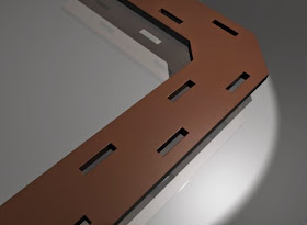
WHY SLOTTING ??
In Deep Sub-micron ULSI integrated circuits, the interconnect structures suffer from various reliability issues - one is the mechanical stress .
Excessive mechanical stress causes ‘passivation-cracking’, ‘metal & dielectric-cracking’, ‘void-formation’, and ‘extrusions which might cause
shorts’. Mechanical stress develops in metal interconnects – mainly due to
- mass transport [Electromigration, that causes both voids and extrusions , will not be discussed in this document]
- thermal stress [Metal slotting is the technique, used to relieve or control damages caused by thermal stress ]
- other manufacturing issues, and
- chip packaging.
During chip processing, the metal deposition that happens on a heated substrate undergoes void formation [fi rst reported in 1984, on Al
interconnects] happens during cooling [condensation after vapor phase]. During the initial phase, thermally activated dislocations [known as
plastic deformation] which is driven by shear stresses, due to di fferent thermal expansion/compression coefficient cient of metal relative to
surrounding dielectrics and passivation structures. The magnitude of the overall stress depends on extent of oxide con nement, and is a
function of thickness and width of metal lines. Metal slotting, i.e. cutting away rectangular pieces of metal [sometimes called cheesing] from
wide and large metal lines keeps the thermal stress under control [ stress-relief].
Rules for metal-slotting are also called Stress-relief-rules. These rules are foundry & process specific. In other words, metal-slot rules for foundry-A, will be different across their own manufacturing processnodes for example, 65nm, 0.13um, 0.35um SiGe all have their specific slotting guidelines. The rules might not be same for the same manufacturing node across different foundries.
However, following are typical set of rules used :
Slotting-criteria: As only wide metals are slotted, it starts with identification of wide-metal-pieces.
- Wide metals are defined in terms of width and length of metal-region. If the metal region, is wider than a specified dimension [ roughly 4 times the min-width] , and longer than minimum length criteria, it is slotted.
Metals that belong to dummy or fill-pattern, are excluded.
- Metal-resistor regions are excluded.
- Bond-pad regions are excluded.
- Design [IP] that already are DRC clean and pre-characterized are usually excluded.
Slotting-constraints:
a. The slots [holes] have a minimum and maximum dimension [ both length & width ]
b. Spacing between slots [ different dimension between coaxial & parallel slots ]
c. Clearance from the metal boundary
d. Offset between staggered slots
e. slot to line-end clearance
f. Min distance between Slot to VIA [ no slotting over VIA ]
g. VIA-array regions are treated differently for current crowding reasons,. Minimum separation of slot
from via-array
h. Rectangular slots should be ideally aligned with the current direction - opposite is prohibitive. *
* As during DRC stage, current directions are not known, geometric alignment approach is used - length of slots along the length of the metal piece is used. However for “L-shaped” and “T shaped” metals and large complex interconnect shapes, it might be required to fracture them and work with vertical and horizontal metal regions separately. 45-degree regions are avoided. At times, it is only recommended to slot the power-lines.


Amazing work!! make more of this type of blog EN8 CARBON STEEL
ReplyDeletegerman language a1 level is the beginner stage of German learning, where students understand basic words, simple sentences, and everyday expressions, and can introduce themselves, ask simple questions, and communicate in daily situations with basic grammar and vocabulary.
ReplyDelete