Tuesday, 7 April 2015


Short Circuit Power
When dynamic power is analyzed the switching component of power consumption, an instantaneous rise time was assumed, which insures that only one of the transistors is ON. In practice, finite rise and fall times results in a direct current path between the supply and ground, GND, this exists for a short period of time during switching.

Short circuit power [3]
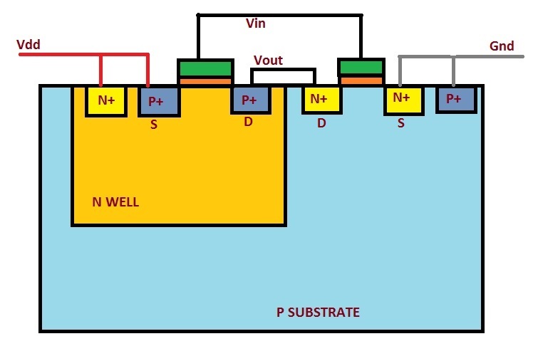
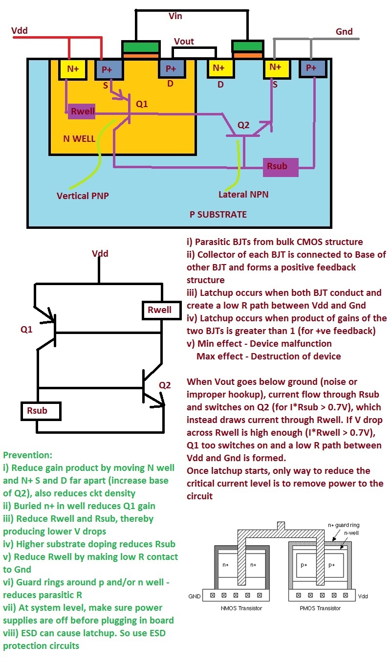
Consider an example of inverter. During switching both NMOS and PMOS transistors in the circuit conduct simultaneously for a short amount of time. Specifically, when the condition, VTn (lesser than) Vin (lesser than) Vdd - |VTp| holds for the input voltage, where VTn and VTp are NMOS and PMOS thresholds, there will be a conductive path open between Vdd and GND because both the NMOS and PMOS devices will be simultaneously on. This forms direct current path between the power supply and the ground. This current has no contribution towards charging of the output capacitance of the logic gate.
When the input rising voltage exceeds the threshold voltage of NMOS transistor, it starts conducting. Similarly until input voltage reaches Vdd-|Vt,p| PMOS transistor remains ON. Thus for some time both transistors are ON. Similar event causes short circuit current to flow when signal is falling. Short circuit current terminates when transition is completed.
Assuming symmetric inverter with Kn=Kp=K and Vt,n=|Vt,p|=Vt and very small capacitive load and both rise and fall times are same we can write,
Pavg(short circuit) = 1/12.k.τ.Fclk.(Vdd-2Vt)3 [1]
Thus short circuit power is directly proportional to rise time, fall time and k. Therefore reducing the input transition times will decrease the short circuit current component. But propagation delay requirements have to be considered while doing so.
Short circuit currents are significant when the rise/fall time at the input of a gate is much larger than the output rise/ fall time. This is because the short-circuit path will be active for a longer period of time. To minimize the total average short-circuits current, it is desirable to have equal input and output edge times [2]. In this case, the power consumed by the short-circuit currents is typically less than 10% of the total dynamic power. An important point to note is that if the supply is lowered to be below the sum of the thresholds of the transistors, Vdd (lesser than) VTn + |VTp|, the short-circuit currents can be eliminated because both devices will not be on at the same time for any value of input voltage.
References
[1] Sung Mo Kang and Yusuf Leblebici, “CMOS Digital Integrated Circuits-Analysis and Design”, Tata McGraw Hill, Third Edition, New Delhi, 2003
[2] Anantha P. Chandrakasan, Samuel Sheng and Robert W.Broadersen, “Low Power CMOS Digital Design”, IEEE Journal of Solid State Circuits, vol. 27, no. 4, pp. 472-484, April 1992
[3] Michael Keating, David Flynn, Robert Aitken, Alan Gibsons and Kaijian Shi, “Low Power Methodology Manual for System on Chip Design”, Springer Publications, NewYork, 2007, www.lpmm-book.org, 4/9/2007
Dynamic and Internal Power
Dynamic Power
As the name indicates it occurs when signals which go through the CMOS circuits change their logic state. At this moment energy is drawn from the power supply to charge up the output node capacitance. Charging up of the output capacitance causes transition from 0V to Vdd. Considering an inverter example power drawn from the power supply is dissipated as heat in pMOS transistor. On the other hand charge down process causes NMOS transistor to dissipate heat.
Output capacitance of the CMOS logic gate consists of below components:
1) Output node capacitance of the logic gate: This is due to the drain diffusion region.
2) Total interconnects capacitance: This has higher effect as technology node shrinks.
3) Input node capacitance of the driven gate: This is due to the gate oxide capacitance.

EVDD= 0->∞∫I. VDD(t).VDD.dt∞∫ I.
Therefore energy stored in capacitor is= CL.VDD2 / 2.
This implies that half of the energy supplied by the power source is stored in CL. The other half has been dissipated by the PMOS devices. This energy dissipation is independent of the size of the PMOS device. During the discharge phase the charge is removed from the capacitor, and its energy is dissipated in the NMOS device.
If a gate is switched on and off ‘fn’ times / second, then Pdynamic = CL. VDD2. fn.
Where fn à frequency of energy consuming transitions. This is also called "switching activity".
In general we can write,
i.e. Pavg=1/T Cload.VDD2
i.e. Pavg=Cload.VDD2.Fclk
Dynamic Power
As the name indicates it occurs when signals which go through the CMOS circuits change their logic state. At this moment energy is drawn from the power supply to charge up the output node capacitance. Charging up of the output capacitance causes transition from 0V to Vdd. Considering an inverter example power drawn from the power supply is dissipated as heat in pMOS transistor. On the other hand charge down process causes NMOS transistor to dissipate heat.
Output capacitance of the CMOS logic gate consists of below components:
1) Output node capacitance of the logic gate: This is due to the drain diffusion region.
2) Total interconnects capacitance: This has higher effect as technology node shrinks.
3) Input node capacitance of the driven gate: This is due to the gate oxide capacitance.

EVDD= 0->∞∫I. VDD(t).VDD.dt
=VDD. 0->∞∫ CL.(dvout/dt).dt
= CL.VDD. 0->VDD∫.dvout
= CL.VDD2
Ec = 0->∞∫ I.
= 0->∞∫ CL.(dvout/dt).vout.dt
= CL.(integration from 0 to VDD).Vout.dvout
= (CL.VDD2)/2
Therefore energy stored in capacitor is= CL.VDD2 / 2.
This implies that half of the energy supplied by the power source is stored in CL. The other half has been dissipated by the PMOS devices. This energy dissipation is independent of the size of the PMOS device. During the discharge phase the charge is removed from the capacitor, and its energy is dissipated in the NMOS device.
If a gate is switched on and off ‘fn’ times / second, then Pdynamic = CL. VDD2. fn.
Where fn à frequency of energy consuming transitions. This is also called "switching activity".
In general we can write,
Pdynamic = Ceff.VDD2.f
Where f à maximum switching activity possible i.e. clock rate.
Hence,
Pavg= 1/T [0->T/2∫Vout (-Cload.dVout/dt)dt+T/2->T∫(VDD-Vout)(Cload.dVout/dt) dt]
i.e. Pavg=1/T Cload.VDD2
i.e. Pavg=Cload.VDD2.Fclk
Here energy required to charge up the output node to Vdd and charge down the total output load capacitance to ground level is integrated. Applied input periodic waveform having its period T is assumed to be having zero rise and fall time. Note that average power is independent of transistor size and characteristics.
Internal power
This is the power consumed by the cell when an input changes, but output does not change [3]. In logic gates not every change of the current running through an input cell necessarily leads to a change in the state of the output net. Also internal node voltage swing can be only Vi which can be smaller than the full voltage swing of Vdd leading to the partial voltage swing.
1) Reduce power supply voltage Vdd
2) Reduce voltage swing in all nodes
3) Reduce the switching probability (transition factor)
4) Reduce load capacitance
This is the power consumed by the cell when an input changes, but output does not change [3]. In logic gates not every change of the current running through an input cell necessarily leads to a change in the state of the output net. Also internal node voltage swing can be only Vi which can be smaller than the full voltage swing of Vdd leading to the partial voltage swing.
Below mentioned steps can be taken to reduce dynamic power
1) Reduce power supply voltage Vdd
2) Reduce voltage swing in all nodes
3) Reduce the switching probability (transition factor)
4) Reduce load capacitance
1) Reduce power supply voltage Vdd
2) Reduce voltage swing in all nodes
3) Reduce the switching probability (transition factor)
4) Reduce load capacitance
Dynamic (switching) power
As we seen in earlier blog the average power consumed by the CMOS circuit can be devided into three different components. They are:
1)Dynamic (switching)power consumption
2)Short circuit power consumption
3)Static (Leakage) power consumption========================================================================
Dynamic (switching) power dissipation
As the name indicates it occurs when signals which goes through the CMOS circuits change their logic state. At this moment energy is drawn from the power supply to charge up the output node capacitance.Charging up of the output capacitance causes transition from 0V to Vdd.Considering an inverter example power drawn from the power supply isdissipated as heat in pMOS transitor. On the other hand charge down process causes NMOS
transistor to dissipate heat. Output capacitance of the CMOS logic gate consists of
below components:
1)Output node capacitance of the logic gate: This is due to the drain diffusion region.
2)Total interconnect capacitance: This has higher effect as technology node shrinks.
3)Input node capacitance of the driven gate: This is due to the gate oxide capacitance.
To find the avearage power energy required to charge up the output node to Vdd and charge down the total output load capacitance to ground level is integrated. Applied input periodic waveform having its period T is assumed to be having zero rise and fall time. Note that average power is independent of transistor size and characteristics.
Internal power
This is the power consumed by the cell when an input changes, but output does not change. In logic gates not every change of the current running through an input cell necessarily leads to a change in the state of the output net. Also internal node voltage swing can be only Vi which can be smaller than the full voltage swing of Vdd leading to the partial voltage swing.
======================================================
How to reduce dynamic power?
1)reduce power supply voltage Vdd
2)reduce voltage swing in all nodes
3)reduce the switching probabilty (transition factor)
4)reduce load capacitance
=======================================================
Reference:
[1] Sung Mo Kang and Yusuf Leblebici, CMOS digital integrated circuits-analysis and design, Tata McGraw hill, third edition, 2003
[2]Astro User Guide, Version X-2005.09, September 2005
=======================================================
Different Types of Power Consumption in CMOS Circuits
The average power consumed by the CMOS circuit can be divided into threedifferent components. They are:
1) Dynamic (switching)power consumption
2) Short circuit power consumption
3) Static (Leakage) power consumption
3) Static (Leakage) power consumption
Detail discussion on these topics we will see in coming blogs !
=======================================================
Reference:
[1] Sung Mo Kang and Yusuf Leblebici, CMOS digital integrated circuits-analysis and design, Tata McGraw hill, third edition, 2003
=======================================================
Monday, 6 April 2015
Advanced Clock Tree Synthesis
Reducing Power with Advanced Clock Tree Synthesis:
Clock trees pose a growing
challenge to advanced node IC design, particularly with regard to the chip
power consumption. Clocks are the single largest source of dynamic power usage,
which makes clock tree synthesis (CTS) and optimization as a good place to
achieve significant power savings.
In today’s leading-edge designs,
CTS is further complicated by two relatively recent developments: the explosion
in the number of modes, corners, and power domains across which the clock must
operate, and the increasing resistance and variation in resistance between
design corners.
Multiple Modes, Corners, Power Domains Impact Clock Power:
Variability associated with multiple design modes, process corners, and power states makes balancing clocks more challenging than ever. Using a CTS engine that cannot efficiently and accurately represent more than a couple of mode/corner scenarios leads to errors due to multiple manual CTS runs, longer design times, and lost performance and power because of over-buffering and over-margining required when mode/corner/voltage scenarios are processed serially.Process Scaling Effects on Clock Power :
At smaller geometries, resistance per unit length of interconnect is rapidly increasing when compared to capacitance, and if not addressed, could impact circuit performance and clock trees. In addition to the increasing resistance, the variation of these values is also increasing.Low-Power CTS Techniques:
Clock power consumption is a factor
of capacitance, switching activity, and wire length. Low-power CTS strategies
include lowering overall capacitance and minimizing switching activity. Some of
the advanced techniques to help address power, and also timing, are listed
below.
- Reducing functional skew and skew across corners by using MCMM CTS
- Lowering leaf cluster capacitance with register clumping and clock gate cloning and de-cloning
- Improving clock gating coverage with netlist-level gating, hierarchical gating and activity based gating
- Minimizing switching activity with smart clock gate placement
Clean up Transition Violations between ICC and PTSI
ABSTRACT
When we talk about SI effect, people always care about delta-delay and noise. But omit another important issue, the transition effort induced from SI. In deep sub-micro designs, the timing DRC issue, especially transition violation, is much more critical. This paper will introduce two methods to fix transition violations. Firstly, prevent transition violations caused by long net at place or CTS phase in ICC. Secondly, fix transition violations based on PTSI sign-off analysis report at post-route phase.
In default, ICC uses Arnoldi calculation for partial nets in post-route phase due to runtime consideration. It will degrade transition time correlation between ICC and PTSI. ICC is more optimistic than PTSI. Both ICC and PT provide unique TCL based command. It’s easy to interact or write scripts that can be used for both. We successfully speed up clean up transition violations process in our design with these methods to reduce iterations.
WANG Liang wangliang@vimicro.com
HOU Hua Minhouhuamin@vimicro.com
ZHU Kan zhukan@vimicro.com
Vimicro Corporation
1.0 Introduction
This paper is focus on fixing transition issue in ultra deep sub-micron Back-End design. So far, transition is the important point in timing sign-off flow because the transition violation will affect cell delay calculation, as we known that the cell delay calculation is based on input transition and output load. The transition violation means the transition time value extends the library look up table (which is simulated by library vendor). So the cell delay will be inaccurate and induce risk for tapeout.
Fortunately ICC can help us to deal with most of transition issues, but sometimes, maybe we need some skills or other tools (like PTSI) co-work to speed up transition fixing progress. Generally, in our design, the bottleneck of fixing max transition is caused by two reasons. First, long net connection, it will induce potential transition issue. Secondly, according to runtime, ICC default use Arnoldi calculation for partial nets in post-route phase. It will degrade transition time correlation between ICC and PTSI. ICC is more optimistic than PTSI.
This paper will introduce VIMICRO transition fixing methodology based on ICC and PTSI which include two progresses. At pre-route stage solve the transition issue by fixing the long net connections. At post-route stage fix the remaining transition violations according to the PTSI sign-off DMSA report.
2.0 Clean up transition violations methodology based on ICC and PTSI
Aiming at the reasons of transition violations we import two optional steps with two VIMICRO property procedures: tproc_fix_long_nets and tproc_fix_transition.
One is focusing on fixing long net at early stage of physical implementation to solve some special floorplan requirements such as long channel area. It can be introduced at place or CTS stage.
The other is focusing on SI induced transition violations at sign-off stage which are hard to be fixed in the ICC because of the timing driven engine (according to runtime, ICC default use Arnoldi calculation for partial nets in post-route phase). It will read PTSI DMSA timing DRC report and generate ICC ECO scripts to solve this issue.
Figure 1 shows the situations of these two optimal steps in the normal flow.

2.1 Pre-route potential transition issue
In some special design case, such as long channel area in the floorplan, the calculated result of pre-route signal network load may mismatch with real routing due to long net connections.
Our design includes two power domains. The Always on domain is around shut down domain. There is no way to avoid long channel area in the floorplan like Figure 2.
Sometimes ICC estimates long net load optimistically and is hard to find a good location to fix long net issue in pre-route phase. It will induce big transition violation in post-route phase and degrade correlation between pre-route and post-route phase.

2.2 Auto fix long net connection at early stage for better transition QoR
It is better if we can solve the long net connection issue before routing, but how to do? The best method is to insert buffer along the real routing. We can separate four steps for it.
Step 1: To find long connection nets in the design.
Step 2: To route the nets which are found in step 1.
Step 3: To insert buffer along the nets which are routed at step 2.
Step 4: To remove the net shapes which are routed at step 2.
Real design may have a lot of long net connections. We wish this dirty job can be done automatically. Based on Synopsys Pilot, we can add procedure to boost up our design environment easily. The procedure tproc_fix_long_nets focuses on long net connection issue in ICC environment. It includes several options such as indicating in which sub module the long net issue will be fixed, the long net threshold, insert buffer distance, buffer type and so on.
Below are this command’s detailed options and usage examples:
tproc_fix_long_nets
-insts “full hier instance names” required
-net_length “max net length” optional
-buf_length “insert buf length” optional
-path “output dir” optional
-file “output file name” optional
-clk_buffer “clock buffer” optional
-nom_buffer “normal buffer” optional
-noroute “the preroute stage” optional
-pre_cts “the pre_cts stage” optional
Usage: tproc_fix_long_nets -insts $TEV_FIX_LONG_NET_MODULES -noroute -pre_cts
Limitation: This procedure can handle clock network at post-CTS stage regardless clock skew. We must run an incremental clock tree optimization to recover clock skew if using this procedure to deal with clock network.
The Figure 3 shows an example of long net connection issue in our design.

The Figure 4 is our procedure result after fixing long net connection issue.

From the result we can easily identify the effect of this method. The long net connection has a lot of bad effects like big transition, SI, EM and RC-009 Warning in the STA. The long channel area floorplan is only one reasons resulting long net connection issue, there may also some other causes. However, any long net connection issue can always be solved by this method.
2.3 Post-route transition report difference between ICC and PTSI
When we talk about SI effect, people always care about delta-delay and noise. But omit another important issue, the transition effort induced from SI. In the deep sub-micro process SI effect is more and more heavy. It can result in transition time difference between the driving pin and loading pin on the same net. With the SI effect the transition time will become worse than without. Like Figure 5 shows.
In the STA tools, the Arnoldi algorithm can evaluate SI affected transition. PTSI is a good sign-off STA tool which uses 100% Arnoldi algorithm. It can calculate SI effect exactly, including transition time. However, ICC default uses Arnoldi calculation for partial nets in post-route phase due to runtime consideration.
The most distinguished difference between PTSI full Arnoldi and ICC partial Arnoldi is SI affected transition time. So the ICC reported transition time is more optimistic than PTSI in post-route phase

2.4 Basic method for transition fixing in post-route phase
Firstly, we can fix transition violations with ICC until timing clean or almost clean (include setup/hold, max transition/capacitance and so on). Then dump netlist and SPEF and use PTSI DMSA feature to report timing for all scenarios. There may still a lot of transition violations, but don’t worry, we can fix them directly according to PTSI report in the PT or ICC environment.
Generally, the easiest method for transition fixing is size up driving strength. If no such cell, we can insert a buffer which driving strength is bigger than original. Figure 6 and Figure 7 shows the Size Up and Insert Buffer methods

2.5 Auto fix transition violations according to PTSI DMSA report
Until now we know it is better to fix transition violations according to PTSI result since the ICC is optimistic with default setting and from its result, we may not see the total transition violations induced by SI completely. The methods of transition fixing are Size Up and Insert Buffer.
The PTSI report probably includes a lot of transition violations even when it is almost clean in the ICC. So perhaps we still have many works to do. Fortunately, we can use another procedure to do this. It is procedure tproc_fix_transition which will do the things below serially.
1. Find out all transition violations in the PTSI DMSA report and unique the driving pins.
2. Try to size up the driving cell with same cell type.
3. Try to insert buffer at driving pin with bigger driving strength than driving cell if step 2 failed.
4. Dump Warning info if neither step 2 nor step 3 succeeds.
Below are this command’s detailed options and usage examples:
tproc_fix_transition
-pt_rpt_file “point pt transition report” required
-path “output dir” optional
-file “output file name” optional
-buffer_list “buffer list” optional
-iteration_loops ”search find loops” optional
Usage: tproc_fix_transition -pt_rpt_file $TEV_PTSI_DMSA_TRAN_RPT
Limitation: This procedure just size up or insert a bigger buffer at driving pin, it cannot choose a location to solve long net and big fanout issues. We must solve long net (with previously procedure tproc_fix_long_nets) and big fanout (set max fanout constraint) in early stage.
Below is part of PTSI DMSA transition report before transition fixing with our procedure:
## Violation Types: max_transition
Worst Violator : -0.3681
===================================================
Violation Range for Bar 1 : -0.000000 to -0.073560
Violation Range for Bar 2 : -0.073560 to -0.147120
Violation Range for Bar 3 : -0.147120 to -0.220680
Violation Range for Bar 4 : -0.220680 to -0.294240
Violation Range for Bar 5 : > -0.294240
===================================================
Histogram of violations on (bins = 5)
| (% of WNS) (violations) –>
0-20%: ********************************************* ***** (118)
20-40% : ****************************************** (99)
40-60% : ***************** (40)
60-80% : (1)
> 80% : * (2)
After one iteration loop with tproc_fix_transition procedure, the PTSI DMSA transition report becomes:
## Violation Types: max_transition
Worst Violator : -0.1678
===================================================
Violation Range for Bar 1 : -0.000000 to -0.033560
Violation Range for Bar 2 : -0.033560 to -0.067120
Violation Range for Bar 3 : -0.067120 to -0.100680
Violation Range for Bar 4 : -0.100680 to -0.134240
Violation Range for Bar 5 : > -0.134240
===================================================
Histogram of violations on (bins = 5)
| (% of WNS) (violations) –>
0-20%: ************************ (11)
20-40% : ************************************************** (23)
40-60% : ********* (4)
60-80% : (0)
> 80% : ** (1)
Through about 3~4 iteration loops and a few manual works, we successfully clean up all transition violations in our design.
3.0 Conclusions and Recommendations
With the cooperation of ICC and PTSI we successfully clean up transition violations in our design. At pre-route stage, we use a procedure automatically find and fix long net connection to avoid potential transition violations. At post-route stage, we introduce another procedure which can read PTSI DMSA transition report to automatically fix all remaining transition violations in the ICC or PT environment.
We recommend run incremental clock tree optimization if we need fix long net issue in the clock tree at post-CTS stage to recover clock skew. In post-route phase we recommend fix transition violations in the PT environment based on ‘What-if’ feature. It can evaluate transition fixing effect more quickly
4.0 Acknowledgements
We would like to thank VIMICRO colleagues and Synopsys engineer, our SNUG technical reviewer, for their valuable inputs.
5.0 References
[1] Synopsys, IC Compiler Implementation User Guide, C-2009.06-SP2.
[2] Synopsys, Prime Time User Guide: Fundamentals, B-2008.12.
[3] Synopsys, Prime Time SI User Guide, B-2008.12.
[4] HOU Hua Min, LI Ying, Multi-million Set-Top Box Static Timing Analysis using Distributed Multi-scenario Analysis, Thomson Broadband R&D (Beijing) Co., Ltd, SNUG 2008
Subscribe to:
Posts (Atom)